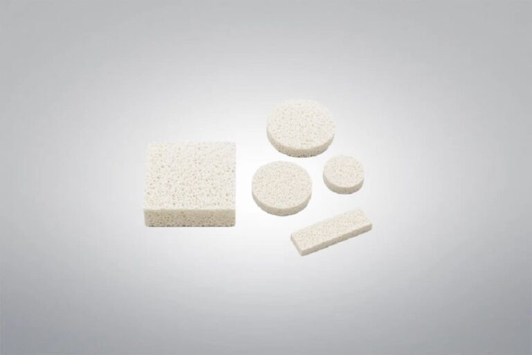
Beryllium Oxide Substrate
Beryllium Oxide Substrate
- Custom sizes and standard sizes in stock
- Quick Lead Time
- Competitive Price
Beryllium Oxide Substrate offers excellent thermal conductivity and electrical insulation, making it ideal for high-performance electronic applications. It supports thick-film metallization through active metal methods such as Mo-Mn or W-Mn, followed by nickel plating and pattern etching to form precise circuits. This makes it widely used in microwave power circuits and integrated circuits where heat dissipation and reliability are critical. As a leading supplier and manufacturer of premium beryllium oxide products, Shanghai Yuepeng can supply high-quality Beryllium Oxide Sustrate with various specifications and competitive prices, offering customized solutions to meet specific requirements.
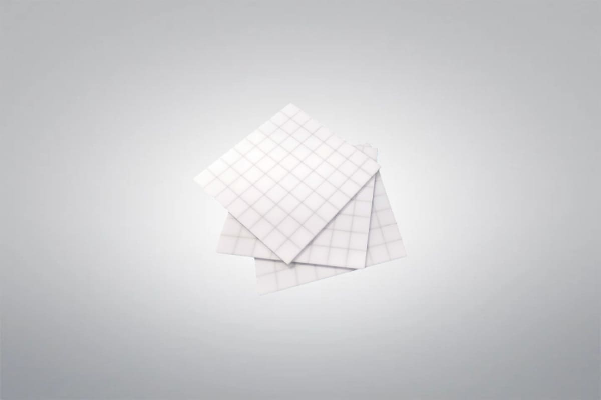
Beryllium Oxide Substrate Data Sheet
| Color: | White |
| Chemical Formula: | BeO |
| Dimension: | customized |
| Machining Accuracy: | 0.01 mm |
| Surface Roughness: | 0.1 μm |
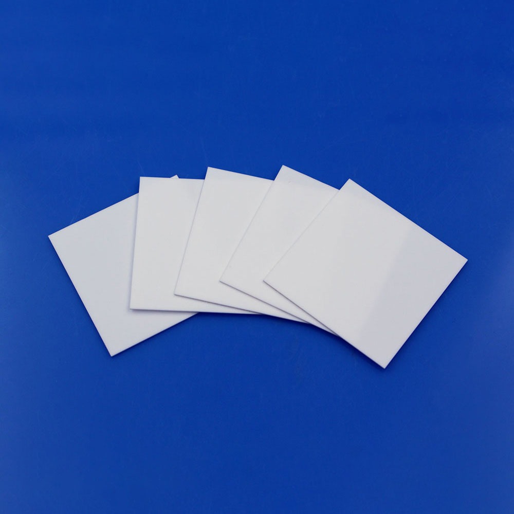
Beryllium Oxide Substrate Description
Beryllium Oxide Substrate, also known as BeO ceramic substrate, is engineered for demanding electronic applications requiring superior heat management and strong dielectric properties. Using active metallization processes like molybdenum-manganese (Mo-Mn) or tungsten-manganese (W-Mn), a robust thick-film metal layer is applied to the surface. After nickel plating and fine-pattern etching, the resulting circuit layer achieves excellent solderability and structural integrity, with tensile strength exceeding 20 MPa. Even under reducing atmospheres at around 800 °C, the nickel layer remains stable without blistering. This makes BeO substrates a dependable platform in high-frequency, high-power electronics, especially in aerospace and telecommunication systems.

Beryllium Oxide Substrate Chemical Compositions
| Element | Content (ppm) |
|---|---|
| Boron (B) | 2 |
| Aluminum (Al) | 46 |
| Chromium (Cr) | 8 |
| Iron (Fe) | 32 |
| Magnesium (Mg) | 1000 |
| Manganese (Mn) | 2 |
| Nickel (Ni) | 9 |
| Titanium (Ti) | 5 |
| Sodium (Na) | 173 |
| Calcium (Ca) | 31 |
| Silicon (Si) | 2100 |
Beryllium Oxide Substrate Features
- Exceptional Thermal Conductivity: Offers outstanding heat dissipation with thermal conductivity up to 280 W/m·K, far exceeding most ceramic materials.
- High Mechanical and Electrical Strength: Combines high dielectric strength with excellent puncture resistance, ensuring stability under demanding electrical loads.
- Low Dielectric Constant and Loss: Maintains low dielectric constant and minimal high-frequency loss, making it ideal for RF and microwave applications.
- Advanced Hot Pressing Process: Manufactured using precision hot-pressing technology, delivering dense, crack-free substrates with consistent quality.
- Flexible Customization: Available in a wide range of shapes, sizes, and thicknesses to meet specific design requirements for power devices and hybrid circuits.
Beryllium Oxide Substrate Applications
- High-Power Electronics: BeO substrates are used in transistors, RF amplifiers, and microwave devices to provide superior heat dissipation while maintaining electrical insulation.
- LED and Optoelectronic Devices: They serve as base materials for LEDs, laser diodes, and photonic devices, ensuring stable thermal management and consistent performance.
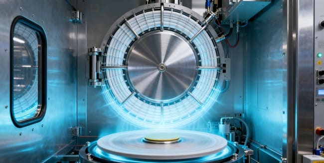
- Semiconductor Components: BeO substrates are applied in wafer processing, chip packaging, and high-frequency circuits, offering dimensional stability and high thermal conductivity under vacuum conditions.
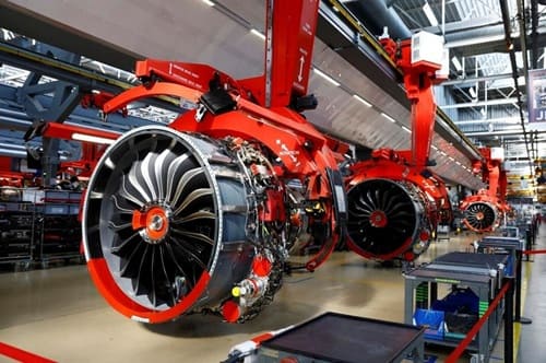
- Aerospace and Defense Electronics: They act as thermal and electrical interfaces in aerospace instrumentation and defense systems, tolerating extreme temperatures and harsh operational environments.
- Medical and Analytical Equipment: BeO substrates are used in imaging devices, sensors, and diagnostic instruments that require efficient heat dissipation, electrical insulation, and reliability in high-performance applications.
 Semiconductor Etching
 Defense and Aerospace
 Medical Devices
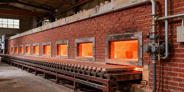
 High-Temperature Furnaces
 Optical and electronic industries


Beryllium Oxide Ceramic Properties
Beryllium Oxide Ceramic Material Machining
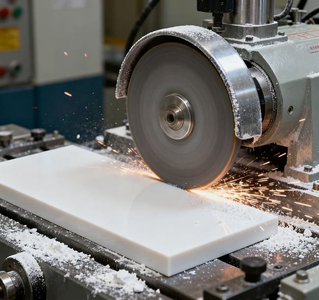
Beryllium Oxide (BeO) Ceramic is valued for its exceptional thermal conductivity, electrical insulation, and high melting point. These qualities make it widely used in electronics and high-temperature applications, but its hardness and brittleness require special machining approaches. Key machining considerations include:
- Cutting: Precision diamond-coated tools or laser cutting are essential to avoid microcracks and maintain clean edges, as BeO’s brittleness can lead to chipping during conventional cutting.
- Grinding: Fine diamond grinding wheels enable accurate shaping and surface finishing while minimizing the risk of fractures, especially important for small or complex parts.
- Drilling: Ultrasonic machining or abrasive waterjet methods are preferred to produce precise holes without causing thermal damage or cracks.
- Surface Finishing: Polishing techniques enhance surface smoothness and electrical insulation properties, crucial for applications demanding high dielectric performance and reliability.
Beryllium Oxide Ceramic Packaging
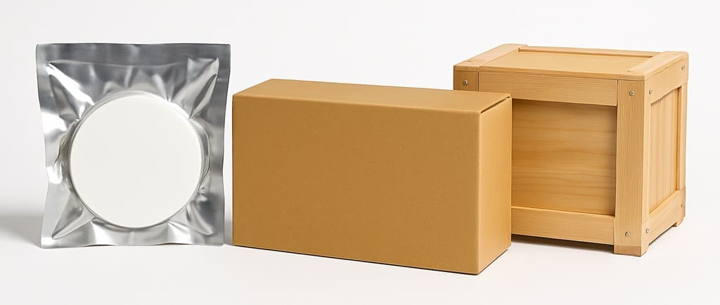
Beryllium Oxide Ceramic products are typically packaged in vacuum-sealed bags to prevent moisture or contamination and wrapped with foam to cushion vibrations and impacts during transport, ensuring the quality of the products in their original condition.
Download
Get A Quote
We will check and get back to you in 24 hours.