
High-Performance Alumina Substrates: Fabrication Techniques and Processing Guidelines
With the rapid development of 5G, the Internet of Things (IoT), and power electronics technology, electronic components are continually evolving towards miniaturization, high integration, and high-frequency high-speed performance. This shift places higher demands on the thermal management, insulation reliability, and signal integrity of circuit packaging materials. Alumina ceramics, with their high mechanical strength, excellent insulating properties, good thermal conductivity (around 20-30 W/(m·K)), low dielectric loss, and outstanding thermal shock resistance and chemical stability, have become indispensable key materials in electronic packaging. Furthermore, due to their wide availability of raw materials, relatively low cost, and mature manufacturing processes, alumina ceramic substrates play a crucial role in various applications, including aerospace, new energy vehicles, industrial control, and consumer electronics.
At Shanghai Yuepeng Tech, we specialize in high-quality alumina substrates with a variety of forms and specifications, ensuring optimal performance for industrial and scientific applications.
Key Performance Metrics for High-Performance Alumina Substrates
Before diving into manufacturing details, it is essential to define what “high performance” specifically entails. These performance metrics are interrelated and collectively determine the substrate’s performance in the end product.
1. Thermal Properties
The core metric is Thermal Conductivity, which measures a material’s ability to conduct heat. For power devices, efficient heat dissipation is paramount.
Influencing Factors:
- Purity: The thermal conductivity of 99.6% Al₂O₃ (~30 W/mK) is significantly higher than that of 96% Al₂O₃ (~20-25 W/mK) because glass phases and other impurities strongly scatter phonons (the primary heat carriers).
- Density: Any residual pores are obstacles to heat flow; thus, a sintered body close to theoretical density is a prerequisite for high performance.
- Grain Boundaries: Grain size and grain boundary properties affect phonon transport. Generally, large and uniform grains are beneficial for thermal conductivity.
2. Electrical Properties
- Insulation Strength: The substrate’s ability to resist breakdown under high voltage, typically required to be > 10 kV/mm.
- Dielectric Constant: Affects signal propagation speed, requiring a stable and appropriate value in high-frequency applications.
- Dielectric Loss: Should be as low as possible to minimize energy loss and heating during signal transmission.
3. Mechanical Properties
- Flexural Strength: Measures the substrate’s resistance to fracture, ensuring mechanical reliability during assembly and use.
- Hardness and Wear Resistance: Important for scenarios involving mechanical contact or grinding processes.
4. Surface Characteristics
- Surface Roughness (Ra): This is critical for the success of metallization processes. Excessive roughness can cause continuity issues in thin-film circuits, while insufficient roughness may result in poor adhesion. Typically, thin-film circuits require Ra < 0.1 μm, while thick-film circuits can tolerate Ra < 0.5-0.8 μm.
- Flatness / Warpage: Affects photolithography accuracy and component mounting precision.
To meet performance requirements, substrates must achieve high purity levels (often >99.5% Al₂O₃), exceptional surface smoothness (Ra < 0.1 μm), and precise dimensional stability (±0.1% tolerance). These standards ensure minimal defects, such as porosity or inclusions, which could compromise functionality. For instance, in high-frequency devices, surface roughness directly impacts signal integrity, while purity affects dielectric losses.
| Property | Typical Value | Significance |
| Thermal Conductivity | 20-30 W/m·K | Enables efficient heat management in dense electronics. |
| Dielectric Strength | >10 kV/mm | Prevents electrical breakdown in high-voltage applications. |
| Flexural Strength | 300-400 MPa | Provides mechanical reliability under stress. |
| Thermal Expansion Coefficient | 7-8 × 10⁻⁶/K | Ensures dimensional stability across temperature ranges. |
| Purity Requirement | >99.5% | Minimizes impurities that could lead to performance degradation. |
Looking for top-quality alumina substrates? Explore Shanghai Yuepeng’s selection.
Core Fabrication Technique: The Tape Casting Process
Tape casting is the preferred technique for producing high-quality, large-area, uniformly thick planar ceramic substrates. It is essentially a slurry-based forming process.
Technique Overview
The process is analogous to “coating paste.” A carefully prepared ceramic slurry (casting slip) with specific rheological properties is spread through a precision doctor blade orifice onto a moving carrier film (e.g., Mylar®) at a uniform thickness. The slurry then passes through a drying zone where volatile solvents evaporate, leaving behind a flexible and mechanically robust “green tape.” This tape can be rolled, cut, and punched like paper, ready for subsequent lamination and sintering.
Slurry Preparation
This is the foundation of the entire process; the formulation determines the quality of both the green tape and the final product. The slurry is a complex multi-component system:
- Ceramic Powder: The main body is alumina powder. Its particle size distribution (PSD) is crucial. A mono-sized powder cannot achieve high packing density. An ideal PSD is bimodal or even multimodal, allowing small particles to fill the gaps between larger ones, resulting in a high-density green body before sintering.
- Dispersant: Its function is to adsorb onto the powder particle surfaces, preventing agglomeration through electrostatic repulsion or steric hindrance, ensuring uniform and stable dispersion in the solvent.
- Binder: After solvent evaporation, it forms a three-dimensional network that provides sufficient mechanical strength to the green tape for handling and machining. Common examples include PVB (Polyvinyl Butyral).
- Plasticizer: Compatible with the binder, it inserts itself between the polymer chains, lowering the glass transition temperature and increasing the flexibility of the green tape to prevent brittle fracture.
- Solvent: Acts as the carrier, dissolving other organic components. Commonly used are azeotropic mixtures like ethanol/toluene or more environmentally friendly alcohol-ether solvents.
The Casting Process
Parameter control is key to ensuring tape uniformity.
- Doctor Blade Gap: Directly determines the wet thickness of the tape, influencing the final thickness after drying and sintering.
- Carrier Speed: Coordinated with the slurry feed rate to ensure a stable “slurry reservoir” forms under the blade.
- Drying Conditions: Temperature and airflow must be strictly controlled. Too rapid drying causes skin formation, leading to bubbles or cracks from internal solvent evaporation; too slow drying reduces efficiency and may cause particle migration, leading to inhomogeneity through the tape thickness.
Critical Post-Processing Steps and Guidelines
The green tape is only a semi-finished product, and subsequent thermal treatment and machining are the “alchemy” that imparts final properties.
Sintering Process
This is the core of ceramic formation, involving two critical stages.
Binder Burnout (Debinding): Before reaching the sintering temperature, the organic additives (binder, plasticizer, etc.) must be completely yet slowly removed from the green body. This process requires extremely careful control of the heating rate (typically very slow, e.g., 0.5-2°C/min), with sufficient holds at critical temperature ranges (e.g., 200-500°C). If heated too quickly, the rapid decomposition of organics generates large volumes of gas, causing blistering, cracking, or even explosion of the body.
High-Temperature Sintering: After debinding, the temperature is raised to the sintering temperature of alumina (typically 1500-1650°C, depending on the formulation). At this stage, atoms gain sufficient energy to diffuse, necks form and grow between particles, pores are gradually eliminated, and the material undergoes significant volume shrinkage (linear shrinkage can reach 15-20%), eventually becoming dense and hard. The sintering profile (temperature-time curve) decisively influences the microstructure.
- Excessive Temperature/Hold Time: Leads to abnormal grain growth. While it might increase thermal conductivity, it severely reduces mechanical strength and is detrimental.
- Insufficient Temperature/Hold Time: Results in incomplete densification, with numerous residual pores, failing to meet performance standards.
Precision Machining and Surface Finishing
Sintered substrates often require precision machining to meet dimensional and surface requirements.
- Laser Cutting: Uses high-precision lasers to cut the sintered large plates into specific shapes required by customers. This is the most common and flexible method.
- Grinding and Polishing: Uses diamond wheels or polishing slurries to machine the substrate surface, controlling its thickness tolerance and surface roughness in preparation for subsequent high-quality thin-film metallization (e.g., sputtering).
- Cleaning: Uses methods like ultrasonic cleaning in deionized water with appropriate cleaners to thoroughly remove particles and contaminants left from the machining process.
Common Defect Analysis
- Warpage: Can be caused by uneven green tape thickness, non-uniform heating during sintering, or improper binder burnout.
- Cracking: Results from excessive drying or sintering rates, or internal stress concentration.
- Pores/Bubbles: Caused by inadequate slurry de-airing or poor control of the burnout process.
The manufacturing of high-performance alumina substrates is a precise science and an art requiring extensive experience. From nanoscale powder selection to millimeter-scale slurry rheology control, to macroscale sintering thermal field management, precise control at every stage is guaranteed for achieving excellent final properties. In summary, the key to success lies in a profound understanding and fine-tuning of the entire “Powder -> Slurry -> Green Tape -> Sintering” chain.
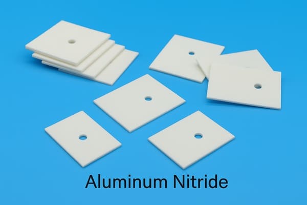
Although materials like Aluminium Nitride have advantages in absolute thermal conductivity, alumina, with its comprehensive cost-performance ratio, technological maturity, and reliability, will remain a mainstay in the field of electronic ceramic substrates for the foreseeable future.
For top-quality ceramic products, Advanced Ceramics Hub provides tailored solutions and precision machining techniques for various applications.
Looking for premium alumina substrate products? Contact us today!